Extremely thin metallic and ceramic layers with high uniformity on square meter panes are now industrial standard. However, the established magnetron sputtering process still faces the constant challenge of reducing costs, improving process stabilization over long periods of time and further simplifying maintenance.
In addition to increasing material utilization, reducing micro-arc discharges and suppressing unwanted dust and particles in the coating sources, the crucial issues are the intelligent interaction between the necessary electrical power supplies and the coating sources.
Target utilization
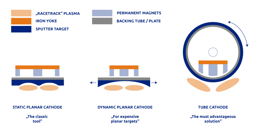 The magnetron sputtering process for the deposition of extremely thin metallic or ceramic layers on flat substrates of up to 18 m² is industrial standard. This means that further improvement in economic efficiency is in the focus of development.
With the introduction of tubular sputtering targets, there was a real boost in terms of material utilization but also in deposition rates. This approach achieves sputter material utilization in the range of up to 80%, a significant improvement compared to approx. 50% with the technically complex dynamic planar cathode and approx. 35% with the static planar cathode.
Process stability
In addition to the sputter material utilization and the deposition rate, another factor is important for the economic viability of the magnetron sputtering process: the so-called arcing.
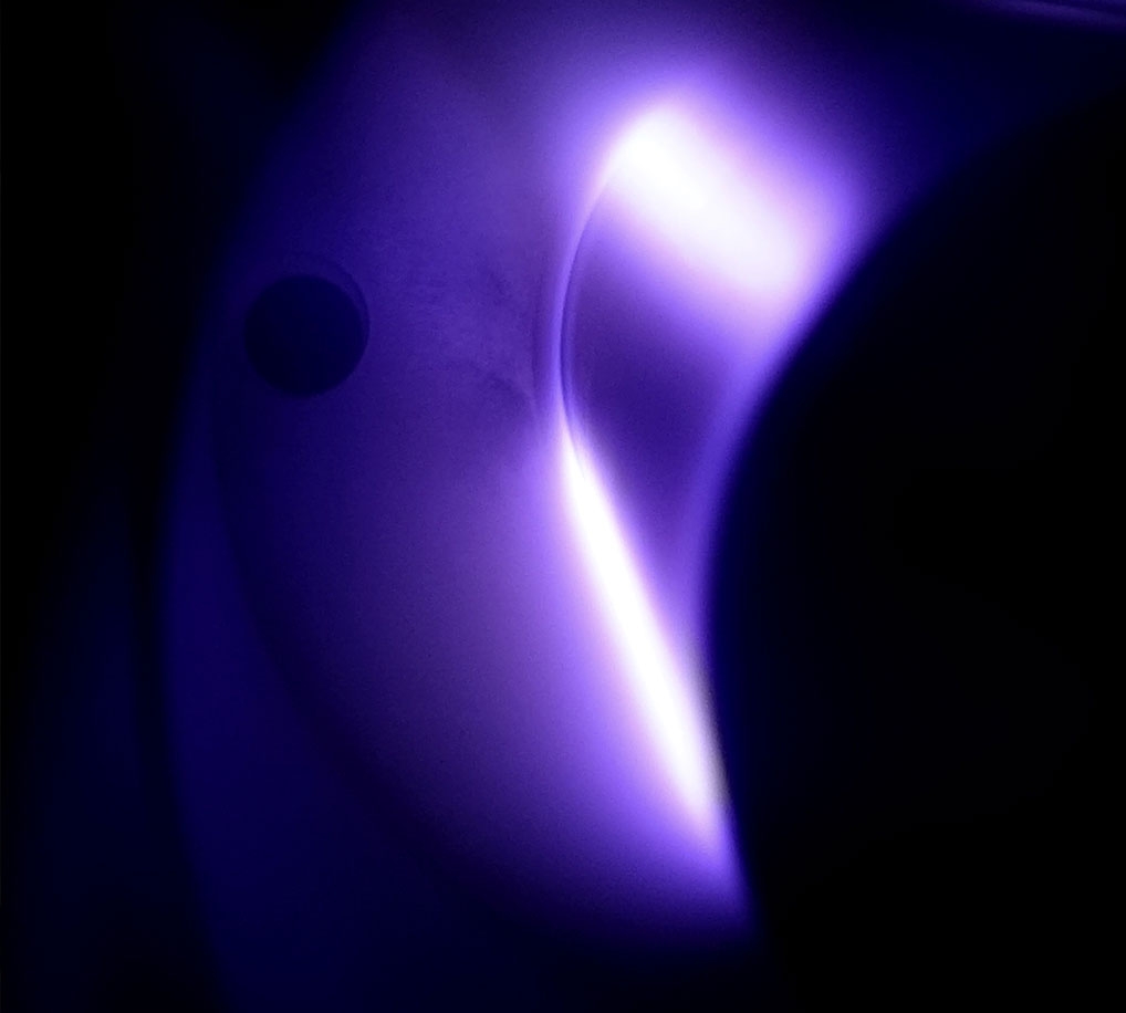
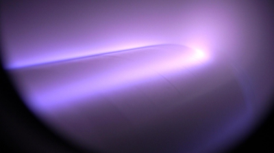
These are not the optically clearly visible, extremely destructive welding arcs, as can be clearly seen in the photos, but rather micro arcs (very limited, barely visible arcs), which can occur at a very high temporal density (several thousand per second) and each lead to the power supply being switched off briefly. This can result in a power supply being “off” half the time to extinguish the numerous micro arcs. The frequency of occurrence of micro arcs is ultimately a question of the material properties of the sputter targets. Depositing dense ceramic or metallic layers with very good layer thickness distribution with minimal “arcing” can only be achieved through clever integration of sputtering cathodes, target material and power supply – the core competence of W&L Coating Systems.

